Charging Regulator
DC-DC Converter
In many industrial applications, it is necessary to convert/modify the value of a direct current (DC) voltage from a source into another DC voltage, which can be either variable or fixed.
A DC converter can convert directly from DC to DC. A DC converter can be likened, by analogy, to an AC transformer (alternating current) that has a variable transformation factor. Like the transformer, the DC-DC converter can be used to step down or step up the output voltage compared to the input voltage 1.
DC-DC converters are used in the following fields:
- traction, in the speed control of motors/servomotors;
- unconventional energies, in battery charging;
- etc..
Depending on the change in output voltage relative to input voltage, in the DC-DC converter, they can be classified as:
- DC-DC buck converter, in English called buck converter;
- DC-DC boost converter, in English called boost converter;
- DC-DC buck-boost converter, in English called buck-boost converter.
These three types of converters are unisolated, meaning that the input voltage and the output voltage share a common point. There are also isolated variations of these converter topologies. The topology of the converter refers to how the switching elements (the transistor, diode, etc.), coil, and output capacitor are connected. Each topology has unique properties. These properties include: the voltage conversion/transformation ratios, the nature of the input and output currents, and the ripple characteristic of the output voltage. Another important property is the frequency response of the transfer function of the output voltage1.
In the following, I will present the three topologies of unisolated DC-DC converters.
The buck DC-DC converter - Buck type1
The most common and probably the simplest topology is the buck type, also known as the buck topology.
Power supply designers choose this topology when the output voltage (or the required/desirable voltage) is lower than the input voltage and the output voltage does not need to be isolated from the input voltage.
The current entering such a topology from the source is discontinuous or pulsating due to the switch, \(Q1\), with current pulsing from \(0\) to \(I_O\) at each switching cycle.
The output current, for a Buck type stage, can be continuous or non-pulsating (without crossing zero), as the output current is supplied by the inductor-capacitor output combination, where the output capacitor never contributes to the output current.
In the figure below, Figure 1, the simplified schematic of a Buck type stage with an included control block is shown.
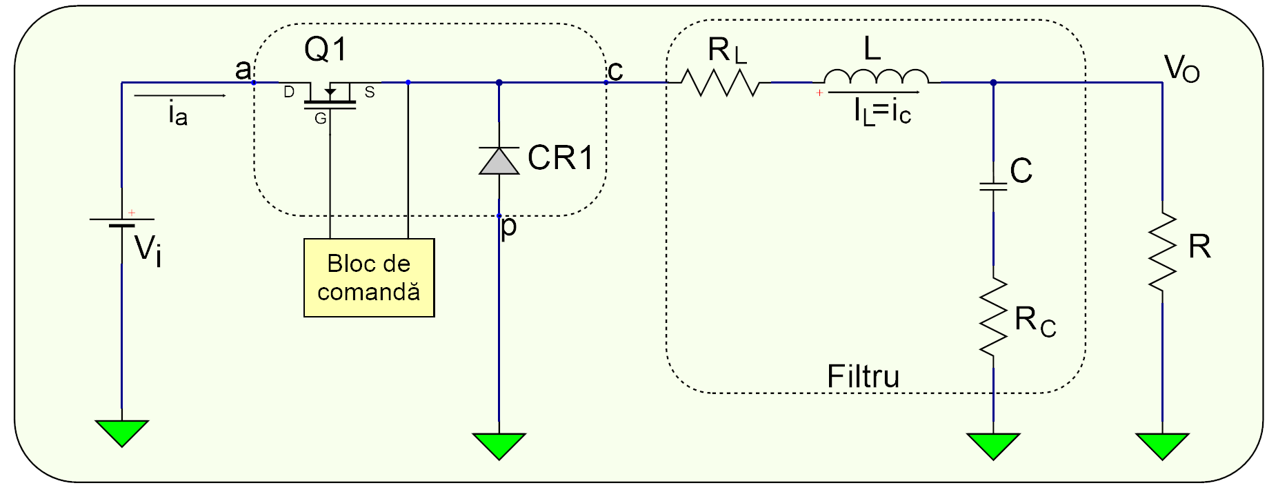
Figure 1. The electrical schematic of a Buck type DC-DC converter.
For analysis, I will use a CAD-type program called LTspice from Analog Devices .
The power switch, \(Q1\), is an N-channel MOSFET transistor, the diode, \(CR1\), is commonly referred to as a catch or freewheeling diode. The inductor \(L\) and capacitor \(C\) form the output filter.

Figure 1a. The electrical schematic of a Buck type DC-DC converter, for simulation with LTspice.
The netlist file of the circuit from Figure 1a is presented below:
* C:\users\florin\Documentele mele\LTspiceXVII\Buck\Buck_2\Buck_2.asc
Vi Vi 0 10
L Vl Vo 50µ Ipk=7 Rser=0.02 Rpar=38000 Cpar=5.86p mfg="Gowanda" pn="894AT5002V"
C Vo 0 100µ V=25 Irms=370m Rser=0.24 Lser=0 mfg="Nichicon" pn="UPL1E101MPH" type="Al electrolytic"
R Vo 0 2
D§CR1 0 Vl RSX051VYM30
V2 Vosc Vl PULSE(0 5 0 1n 1n {DT} {T})
M§Q1 Vi Vosc Vl Vl IRFH5007
.model D D
.lib C:\users\florin\Documentele mele\LTspiceXVII\lib\cmp\standard.dio
.model NMOS NMOS
.model PMOS PMOS
.lib C:\users\florin\Documentele mele\LTspiceXVII\lib\cmp\standard.mos
.tran 0 25m 24.5m
.param D=d T=1/f DT=D*T
.step param d 0.1 0.95 0.1
.param f=50k
.meas TRAN Vo_mediu AVG V(Vo)
.meas TRAN IL_mediu AVG I(L)
.meas TRAN Ic_mediu AVG I(C)
.backanno
.end
The result of the simulation of the above circuit is shown in the image below, Figure 2.
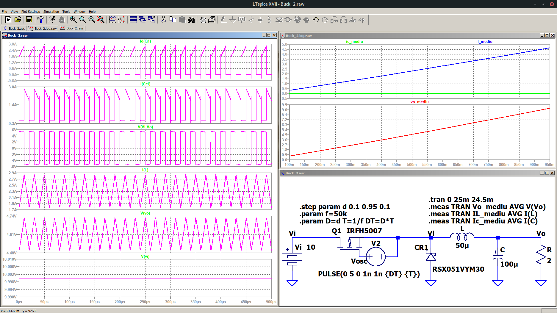
Figure 2a. The waveforms resulting from the simulation of the Buck type c.c. converter, from Figure 1, for \(D=0.5\).
In Figure 3a, the \(ESR\) characteristic of the capacitor, \(C\), is equated with the series resistance, \(Rc\), with it, while the equivalent series resistance of the inductor, \(L\), is equated with the resistance mounted in series with it, denoted as \(RL\). The resistor, \(R\), represents the load seen by the Buck type converter.
For simplification, the transistor, \(Q1\), has been replaced with a voltage-controlled switch, and the conduction resistance, \(RDS\), of the transistor has been taken into account, which is mounted in series with the switch. The schematic is electrically equivalent to the schematic in Figure 1.
The netlist file of the circuit in Figure 3a is as follows:
* C:\users\florin\Documentele mele\LTspiceXVII\Buck.asc
S§Q1 Vl N001 Vosc 0 SW_Q1
Vi Vi 0 10
L N002 Vo 50µ
C Vo N003 100µ
R Vo 0 2
D§CR1 0 Vl RBR20BM30A
V2 Vosc 0 PULSE(0 1 0 0 0 {DT} {T})
RL N002 Vl 0.02
RDS Vi N001 5.9m
Rc N003 0 0.24
.model D D
.lib C:\users\florin\Documentele mele\LTspiceXVII\lib\cmp\standard.dio
.tran 0 10m 9.5m
.model SW_Q1 SW(Ron=0.1 Roff=1Meg Vt=.5 Vh=-.4)
.param D=d T=1/f DT=D*T
.step param d 0.1 0.95 0.1
.param f=50k
.meas TRAN Vo_mediu AVG V(Vo)
.meas TRAN IL_mediu AVG I(L)
.meas TRAN Ic_mediu AVG I(C)
.backanno
.end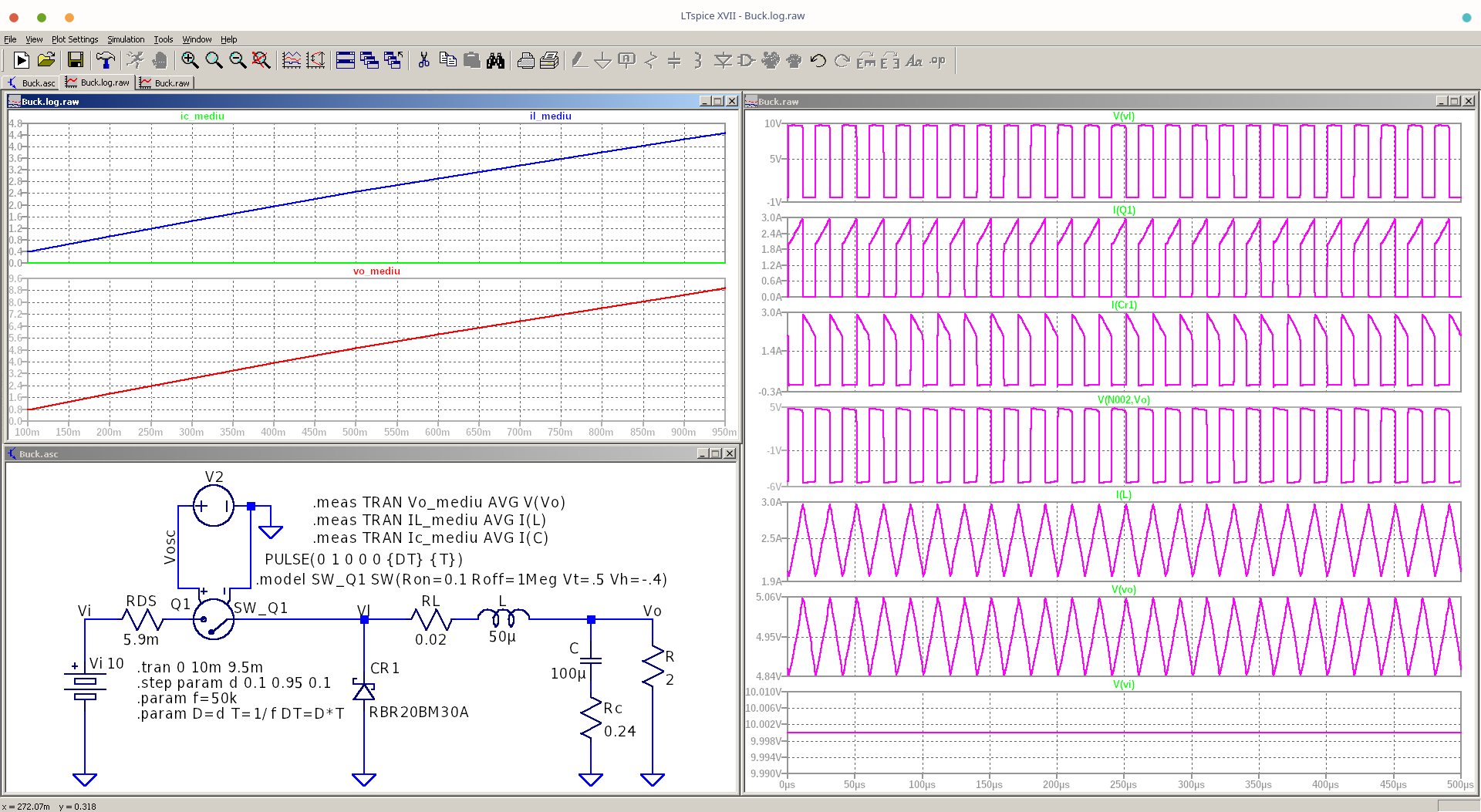
Figure 3a. The waveforms resulting from the simulation of the Buck type c.c. converter, from Figure 1, for \(D=0.5\).
During the normal operation of the DC-DC converter, of the Buck type, the switch \(Q1\) is controlled to be in the closed or open position by the control circuit/block. This action of the control circuit/block on the switch causes the appearance of a pulse train at the intersection of the three elements \(Q1\), \(CR1\), and \(L\), which is filtered by the output filter \(L-C\) to produce a continuous output voltage, \(V_o\).
Static regime (steady state) analysis of the c.c. - c.c. buck converter
Such a converter can operate in discontinuous or continuous current mode (depending on the current through the inductor \(L\)).
Continuous current mode is characterized by the continuous flow of current through the inductor \(L\) throughout the entire switching cycle.
Discontinuous current mode is characterized by the interrupted flow of current through the inductor \(L\), with crossings through zero. This mode is characterized by the fact that the current through the inductor is zero for a portion of the switching cycle. It starts from zero, reaches a maximum value, and returns to zero during each switching cycle.
For this analysis, an N-channel MOSFET transistor is used, which is controlled by a positive voltage \(V_{GS(ON)}\), applied to the gate \(G\) and source \(S\) of the transistor/switch \(Q1\) by the control circuit that commands this switch/transistor \(Q1\) to the \(ON\) position. The advantage of this N-channel MOSFET transistor is that it has a low conductance resistance \(R_{DS(ON)}\), but the control circuit is more complicated. In the case of a P-channel MOSFET transistor, which generally has a higher conductance resistance \(R_{DS(ON)}\), the control circuit is simpler.
The transistor \(Q1\) and the diode \(CR1\) are illustrated in Figure 1, in the dashed box, with terminals labeled a, p, and c. The current through the coil \(L\) denoted as \(I_L\), is the same as the current exiting through the terminal labeled c, namely the current \(i_c\).
The analysis in direct current mode of the DC-DC converter - Buck type
The following describes the operation of the Buck type stage, in static regime (steady state), in direct current operating mode (\(I_L>0\)).
The main result of this analysis is the dependence of the output voltage \(V_o\) on the duty cycle \(D\) and the input voltage \(V_i\).
The static (steady state) regime implies that the input voltage, output voltage, output current through the load, and duty cycle are fixed and do not vary. In general, uppercase letters are assigned to variable names to indicate a quantity in a static state.
In continuous conduction mode, the Buck stage assumes two switching states during a cycle.
- STATE ON - when the transistor/switch, \(Q1\), is \(ON\) and \(CR1\) is \(OFF\);
- STATE OFF - when the transistor/switch, \(Q1\), is \(OFF\) and \(CR1\) is \(ON\).
A simple linear circuit can represent each state in which the elements \(Q1\) and \(CR1\) are replaced with their equivalent circuits corresponding to each state \(ON\) or \(OFF\).
The equivalent electrical schematics for each state are presented in the figure below, Figure 2.


Figure 2. The states \(ON\) and \(OFF\) of the Buck stage.
The duration of the \(ON\) state is:
\[ {T_{ON}}={D} \times {T_S}\]
, where \(D\) is the duty cycle, imposed by the control block, expressed as the ratio of the time when the switch is \(ON\) to the total time of the entire period, \(T_S\):
\[ {D} = {{T_{ON}} \over {T_{S}}}\]
The duration of time for the \(OFF\) state is denoted as \(T_{OFF}\). Thus, we have only two states during the duration of a complete cycle (one period) for continuous current mode. The duration of the \(OFF\) state is:
\[ T_{OFF}=(1-D) \times T_S\]
, where \((1-D)\) is sometimes denoted as \(D'\).
These time cycles are presented in Figure 3.
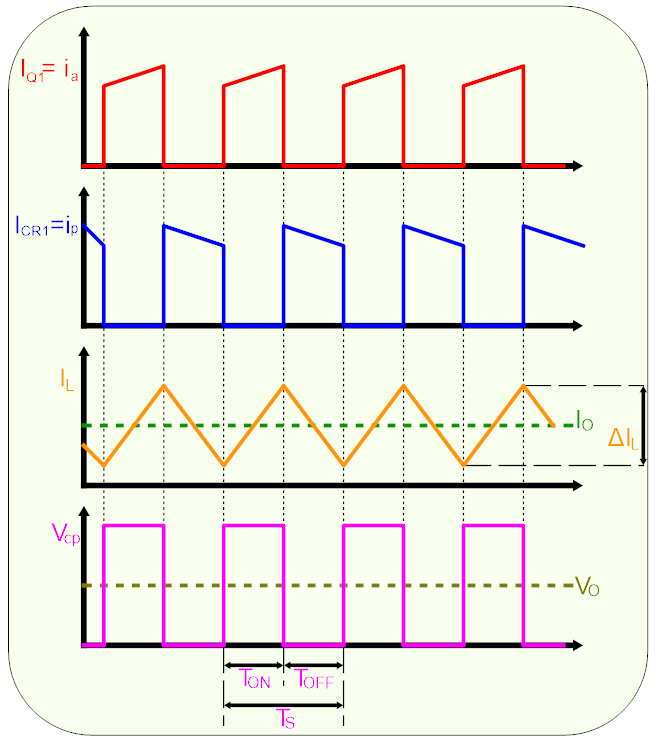
Figure 3. The waveforms in continuous conduction mode, \(I_L>0\).
If we look at Figure 2, during the \(ON\) state, we observe that:
- \(Q1\) exhibits a low resistance, \(R_{DS(ON)}\), from the drain \(D\) to the source \(S\) and has a small voltage drop:
\[ V_{DS}=I_{L} \times R_{DS(ON)}\]
- There is also a small voltage drop across the c.c. resistance of the coil equal to:
\[ V_{RL}=I_L \times R_L\]
Thus, the input voltage, \(V_i\), minus the losses (\(V_{DS}+V_{RL}\)), is applied to the left side of the coil, \(L\). \(CR1\) is \(OFF\) during this time because the applied voltage is reverse. The applied voltage on the right side of the inductor \(L\) is simply the output voltage \(V_o\).
The current through the inductor, \(I_L\), flows from the input source, \(V_i\), through \(Q1\) to the combination of output capacitor, \(C\), and load resistance, \(R\). During the \(ON\) state, the voltage applied across the inductor, \(V_L\), is constant and equal to:
\[ V_L=V_i-V_{DS}- V_{RL} - V_o\]
Adopting the polarity convention for the current \(I_L\) presented in Figure 2, the current through the inductor increases as a result of the applied voltage. Furthermore, since the applied voltage is essentially constant, the current through the inductor increases linearly.
This increase in the current through the inductor during \(T_{ON}\) is illustrated in Figure 3.
\[ {V_L}={L} \times {{di} \over {dt}} \Rightarrow \Delta I_L = {V_L \over L} \times \Delta T \]
The increase in current through the circuit, during the \(ON\) state, is given by:
\[ \Delta I_L(+) = {(V_i - V_{DS} - V_{RL}) -V_O \over L} \times T_{ON} \]
The value \(\Delta I_L(+)\) is the ripple of current through the coil.
If we look at Figure 2, when \(Q1\) is \(OFF\), it presents a high impedance between the drain \(D\) and the source \(S\). Therefore, since the current flowing through the inductor L cannot change instantaneously, the current passes from the transistor \(Q1\) to the diode \(CR1\). As the current through the inductor decreases, the voltage across the inductor reverses polarity until the diode \(CR1\) becomes forward-biased and conducts (\(ON\)).
The voltage on the left side of the coil, \(L\), becomes \(-(V_d+V_{RL})\), where quantitatively, \(V_d\), represents the voltage drop across the diode \(CR1\).
The voltage on the right side of the coil, \(L\), remains the output voltage, \(V_O\).
The current through the coil, \(I_L\), now flows from the ground, through the diode, \(CR1\), to the output formed by the capacitor \(C\) and the load resistor \(R\).
During the \(OFF\) state, the magnitude applied to the coil \(L\) is:
\[ V_L = V_O+V_d+V_{RL}\]
Maintaining the same polarity convention, this applied voltage is negative (or opposite in polarity to the voltage applied in the \(ON\) state).
Therefore, the current through the inductor decreases during the \(OFF\) state.
Also, since the applied voltage is essentially constant, the current through the inductor \(I_L\) will decrease linearly. This decrease in the current \(I_L\) through the inductor during the \(OFF\) state is also presented in Figure 3.
The current through the inductor, during the \(OFF\) state, will decrease according to the relationship:
\[ \Delta I_L(-)={{V_O+(V_d+V_{RL}) \over {L}} \times T_{OFF}} \]
The value of \(\Delta I_L(-)\) is also the ripple of current through the inductor.
In steady state, the current \(\Delta I_L(+)\) increases during the \(ON\) state, and the current \(\Delta I_L(-)\) decreases during the \(OFF\) state. These values must be equal. Otherwise, the value of the current will increase or decrease in net values from one cycle to another, and we are no longer in a steady state.
Therefore, these two equations can be equated and solved for \(V_O\) to obtain the output voltage transformation/conversion relationship \(V_O\) for continuous conduction mode.
Solving:
\[ V_O=(V_i-V_{DS}) \times {T_{ON} \over {T_{ON} + T_{OFF}}}-V_d \times {T_{OFF} \over {T_{ON} + T_{OFF}}} - V_{RL} \]
, where:
\[ \left.\begin{matrix} {T_S=T_{ON}+T_{OFF}} \\ {D={T_{ON} \over T_S}} \\ {(1-D) = {T_{OFF} \over T_S}} \end{matrix}\right\} \Rightarrow V_O=(V_i-V_{DS}) \times D - V_d \times (1-D)-V_{RL}\]
In the above equations for \(\Delta I_L(+)\) and \(\Delta I_L(-)\), the output voltage, \(V_O\), in c.c. was implicitly assumed to be constant, without ripple in voltage during \(ON\) or \(OFF\).
This is a simplification and involves two separate assumptions:
- First, it is assumed that the output capacitor, \(C\), is sufficiently large so that the ripple/voltage change is negligible;
- Second, it is assumed that the voltage drop across the ESR (equivalent series resistance \(R_C\)) is also negligible.
These assumptions hold true because the value of the voltage ripple is designed to be much smaller than the output voltage, \(V_O\), in c.c..
The relationship of the output voltage transformation factor \(V_O\), as mentioned above, illustrates that \(V_O\) can be modified by adjusting the duty cycle \(D\) - also called the fill factor - and is always less than the input voltage \(V_i\) since \(D\) satisfies the condition \(0>D<1\).
Another simplification used is to consider \(V_{DS}\), \(V_d\), and \(R_L\) as implicitly small enough to be ignored, thus:
\[ \left.\begin{matrix} V_{DS}=0 \\ V_d = 0 \\ V_{RL} = 0 \end{matrix}\right\} \Rightarrow V_O = V_i \times D \Rightarrow D={V_O \over V_i}\]
Another simplified way to analyze the operation of the circuit is to consider the output filter as a smoothing network. This is a valid simplification because the cutoff frequency of the filter (usually between \(50[Hz]\) and \(5[kHz]\)) is always lower than the switching frequency of the power supply by \(Q1\) (usually between \(100[Hz]\) and \(500[kHz]\)).
The input voltage applied to the filter is the voltage at the junction of \(Q1\), \(CR1\), and \(L\), denoted as \(V_{c-p}\).
The current through the inductor is equal to the output current since the current through the capacitor is zero.
Mathematically, we have:
\[ I_{L(med)} = I_O\]
The analysis in discontinuous current mode of the c.c. - c.c. buck converter
In the following, we will analyze what happens when the current through the load is low. First, we observe, as shown above, that the Buck stage has the output current \(I_O\) as the average current through the inductor \(I_{L(med)}\).
This is evident because the current \(I_L\) flows through the inductor \(L\) to the capacitor \(C\) and load resistance \(R\), and the average current through the capacitor is zero.
If the current through the output load is reduced below the critical level, the current through the inductor will be zero for a portion of the switching cycle. This should be evident from the waveforms presented in Figure 3, as the peak-to-peak amplitude of the current ripple \(\Delta I_L\) does not change with the output current through the load. In a Buck converter, if the current through the inductor \(I_L\) attempts to drop below zero, it will stop at zero (due to the unidirectional flow of current through the diode \(CR1\)) and remain there until the beginning of a new switching cycle.
This operating mode is called discontinuous conduction mode. A Buck converter operating in this discontinuous conduction mode has three unique states during each switching cycle, unlike the two states for continuous conduction mode.
The load current state when the Buck converter is at the boundary between continuous and discontinuous conduction mode is shown in Figure 4. It can be observed how the current through the inductor falls to zero and the next switching cycle begins immediately after the current reaches zero.
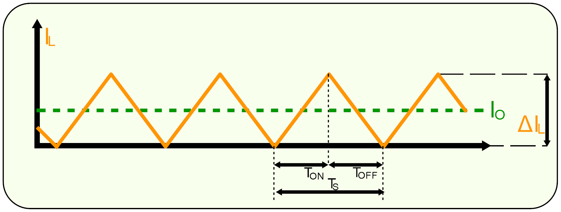
Figure 4. The boundary between continuous conduction mode and discontinuous conduction mode.
The further decrease in output current puts the Buck converter/floor into discontinuous conduction mode. This conduction mode is illustrated in Figure 5. The frequency response of the Buck converter/floor in discontinuous conduction mode is quite different from the frequency response in continuous conduction mode. Additionally, the input-output relationship is quite different, as shown below.

Figure 5. Discontinuous conduction mode.
Before determining the transformation/conversion ratio of the discontinuous conduction mode, we observe that there are three unique states that the Buck converter/floor operates in during the discontinuous current mode:
- The \(ON\) state is when \(Q1\) is \(ON\) and \(CR1\) is \(OFF\);
- The \(OFF\) state is when \(Q1\) is \(OFF\) and \(CR1\) is \(ON\);
- The \(IDLE\) state is when \(Q1\) is \(OFF\) and \(CR1\) is \(OFF\);
The first two states are identical to those of continuous conduction mode, and the circuits in Figure 2 are applicable unless \(T_{OFF} \neq (1-D) \times T_S\). The remaining time is the \(IDLE\) state. Additionally, we will be able to omit: the resistance in c.c. \(R_L\) of the coil/inductor \(L\) implicitly and the voltage drop across it \(V_{RL}\), the voltage drop across the diode \(V_d\), and the voltage drop \(V_{DS}\) across the transistor \(Q1\) in the \(ON\) state, as they are small enough to be considered zero.
The equations for the increase of current, \(\Delta I_L(+)\), through the coil/inductor \(L\) during the \(ON\) state and the equations for the decrease of current, \(\Delta I_L(-)\), through the coil/inductor \(L\) during the \(OFF\) state are determined as follows.
Thus, the increase of current \(\Delta I_L(+)\) through the coil/inductor \(L\), during the \(ON\) state, is given by:
\[ \Delta I_L(+)={{V_i-V_O} \over L} \times {T_{ON}} = {{V_i-V_O} \over L} \times {D \times T_S} = I_{pk} \]
The magnitude of the current ripple, \(\Delta I_L(+)\), is also the peak current, \(I_{pk}\), since in discontinuous conduction mode, the current starts from zero at the beginning of each cycle.
The decrease of the current \(I_L\) through the coil \(L\), during the \(OFF\) state, is given by:
\[ \Delta I_L(-)={{V_O} \over L} \times {T_{OFF}} \]
As in the case of continuous conduction mode, the current increases, \(\Delta I_L(+)\), during the \(ON\) duration and the current decreases \(\Delta I_L(-)\) during the \(OFF\) duration. and these increases and decreases of the current are equal.
Therefore, these two equations can be equated and solved for \(V_O\), to obtain the first of the two equations that must be used to solve the voltage conversion/transformation ratio:
\[ V_O=V_i \times {T_{ON} \over {T_{ON} +T_{OFF}}}=V_i \times {D \over {D+D_2}} \]
The output current, \(I_O\), (the output voltage \(V_O\) divided by the load \(R\)), is the average value of the current, \(I_L\), through the coil \(L\):
\[ I_O=I_{L(med)}={V_O \over R} = {I_{pk} \over 2} \times {{D \times T_S + D_2 \times T_S} \over T_S} \]
Substituting in the equation above \(I_{pk}\) determined earlier, will result in:
\[ I_O={V_O \over R} = (V_i-V_O) \times {{D \times T_S} \over {2 \times L}} \times (D+D_2) \]
Thus, we have obtained two equations, one for the output current, \(I_O\), and one for the output voltage, \(V_O\), both with the terms \(V_i\), \(D\), and \(D_2\).
Now solving each equation for \(D_2\) and equating the two obtained equations. The resulting equation, an expression for the output voltage, \(V_O\).
The voltage conversion/transformation relationship in discontinuous conduction mode is given by:
\[ V_O=V_i \times {2 \over {1+ \sqrt {1+{{4 \times K} \over D^2}}}} \]
, where:
\[ K = {{2 \times L} \over {R \times T_S}} \]
The above relationship presents one of the major differences between the two conduction modes. For the discontinuous conduction mode, the output voltage transformation relationship, \(V_O\), is a function of the input voltage, \(V_i\), the cycle duration (duty cycle), \(D\), inductance \(L\), switching frequency \(T_S\), and load resistance \(R\), while for the continuous conduction mode, the output voltage transformation/conversion relationship depends only on the input voltage, \(V_i\), and the duty cycle (cycle duration), \(D\).
It should be noted that the operating state of a Buck converter/floor, under normal conditions, is rarely in discontinuous conduction mode, but this conduction mode can occur at any time as a result of the load/output current dropping below a certain critical level.
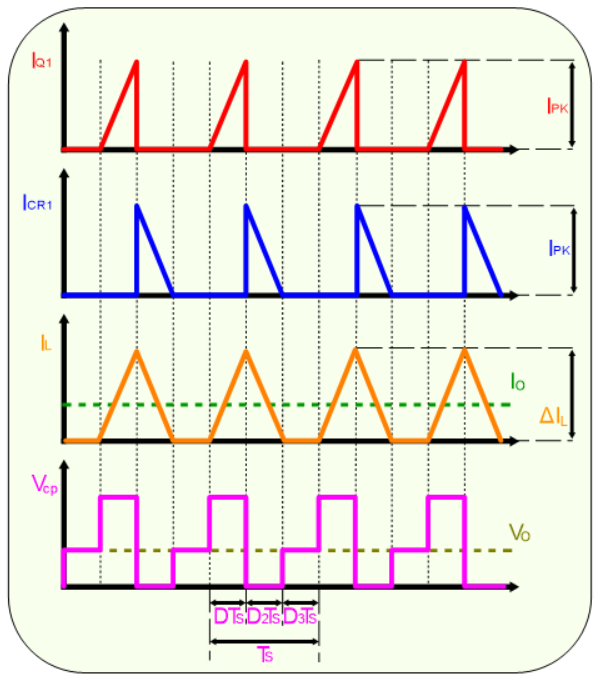
Figure 6. Waveforms in discontinuous conduction mode
Critical inductance
The previous analyses of the Buck converter have been for continuous and discontinuous conduction modes in static regime.
The conduction mode of the converter is a function of the input voltage, output voltage, output current, and the inductance value associated with the output coil.
A Buck converter can be designed to operate in continuous mode for load currents above a certain level, typically 5%-10% of the maximum value.
Typically, the input voltage range, output voltage, and load current are imposed (defined) parameters of the Buck converter, while the value of the inductor is a parameter that needs to be determined in order to maintain the continuous conduction mode.
The minimum value of the inductor to maintain continuous conduction mode can be determined by following the subsequent algorithm.
To begin, we define \(I_{O(crit)}\) as the minimum current for which continuous operation can still be maintained, as shown in Figure 4, and which can be calculated as follows:
\[ I_{O(crit)}= {{\Delta I_L} \over {2}} \]
After which we determine the minimum inductance of the coil (inductor) that satisfies the above relationship, as follows:
\[ L_{min} \geq {1 \over 2} \times (V_O+V_d+V_{RL}) \times {T_{OFF(max)} \over I_{O(crit)}} \]
The above equation can be simplified and arranged in a more usable form:
\[ L_{min} \geq {{V_O \times \left (1-{{V_O} \over V_{i(max)}} \right ) \times T_S} \over {2 \times I_{O(crit)}}} \]
Using the inductance value thus calculated ensures operation in continuous mode for load/output currents above the critical current level, \(I_{O(crit)}\).
Calculation of the components of a Buck converter
The following presents an algorithm for calculating the sizing of a Buck converter that will operate in continuous conduction mode.
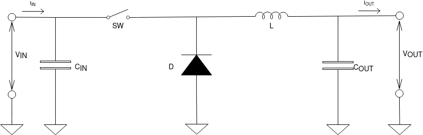
Figure 7. Schematic diagram of a Buck converter
Necessary parameters (known)
for sizing a Buck converter (as shown in the figure above) the following four parameters are required:
- \(V_{IN_{(min)}}\) and \(V_{IN_{(max)}}\), the input voltage range;
- \(V_{OUT}\), the nominal output voltage;
- \(I_{OUT_{(max)}}\), the maximum output current;
- The datasheet of the IC (integrated circuit) used in the construction of the Buck stage, from which certain parameters will be used.
Determining the maximum switching current
In order to determine the maximum switching current, it is necessary first to determine the duty cycle \(D\) for the maximum input voltage, as this evidently imposes the maximum switching current:
\[ D={V_{OUT} \over {V_{IN_{(max)}} \cdot \eta}} \]
where:
\(V_{OUT}\) - represents the output voltage;
\(V_{IN_{(max)}}\) - represents the maximum input voltage;
\(\eta\) - represents the efficiency of the Buck stage.
It is necessary to take into account the efficiency, \(\eta\), to cover the losses of the Buck stage. When this is not known from the datasheets, it can be estimated that if we consider an efficiency of 90%, we will cover the losses within the Buck stage.
The next step in determining the maximum switching current is to determine the current ripple through the inductor. In the datasheet of the converter, the specific value of the inductor or a series of coils (inductors) that can be used in the application of the IC (integrated circuit) is normally specified.
In determining the current ripple (ripple current) through the inductor, we will use the inductance value from the middle of the recommended range, or if this parameter is not specified, we will use the value determined in the next section - Choosing the inductor.
\[ \Delta I_L = {({{V_{IN_{(max)}}-V_{OUT}}) \cdot D} \over {f_s \cdot L}}\]
where:
\(V_{IN_{(max)}}\) - represents the maximum input voltage;
\(V_{OUT}\) - represents the desired output voltage;
\(D\) - duty cycle, determined previously;
\(f_s\) - the minimum switching frequency of the converter;
\(L\) - the value of the inductor's inductance.
In the following, it will be determined whether the integrated circuit (IC) containing \(SW\) can provide the maximum output current (switching current).
\[ I_{MAXOUT} = {I_{LIM_{(min)}}-{\Delta I_L \over 2}} \]
where:
\(I_{LIM_{(min)}}\) - represents the minimum value of the limit current associated with the switching element \(SW\), from the catalog data;
\(\Delta I_L\) - represents the ripple current calculated previously.
If the calculated value of the maximum output current, \(I_{MAXOUT}\), is less than the required maximum output current, then we will increase the switching frequency, \(f_s\), to reduce the ripple current, \(\Delta I_L\), or a switch with a higher output current will be chosen. If the maximum output current, \(I_{MAXOUT}\), is only slightly less than the required maximum output current, then we will increase the inductance of the inductor, \(L\), if we are within the recommended range of the inductor. It can be observed from the previous equation of the current ripple \(\Delta I_L\) that by increasing the inductance, \(L\), or increasing the switching frequency, \(f_s\), the current ripple \(\Delta I_L\) can be reduced, and consequently, the maximum output current, \(I_{MAXOUT}\), will increase.
If the calculated value of the maximum output current, \(I_{MAXOUT}\), exceeds the maximum required output current, then the maximum switching current, \(I_{SW_{(max)}}\), will be calculated using the formula:
\[ I_{SW_{(max)}} = {\Delta I_L \over 2} + I_{OUT_{(max)}} \]
where:
\(\Delta I_L\) - represents the ripple current through the coil (inductor);
\(I_{OUT_{(max)}}\) - represents the maximum current required at the output.
\(I_{SW_{(max)}}\) - represents the maximum switching current, which is the peak current that the switch element, \(SW\), the inductor, \(L\), and the diode, \(D\), must withstand.
Choosing the inductor
The datasheets for the Buck converter often provide a series of recommended values for the inductor. In this case, we can choose the coil (inductor) to have an inductance value from the list of values or a specific model indicated.
From the previous formulas, it can be concluded that the greater the value of the inductance of the coil, \(L\), the greater the maximum output current, \(I_{MAXOUT}\), due to the reduction of the current ripple, \(\Delta I_L\). Additionally, the maximum current supported by the inductor, \(L\), chosen must be greater than the maximum switching current, \(I_{SW_{(max)}}\).
For cases where a specific list of inductors is not provided in the catalog sheets, the following equation can be used to select the required inductance:
\[ L={{V_{OUT} \cdot (V_{IN} - V_{OUT})} \over {\Delta I_L \cdot f_s \cdot V_{IN}}} \]
where:
\(V_{IN}\) - represents the input voltage;
\(V_{OUT}\) - represents the nominal output voltage;
\(f_s\) - represents the switching frequency of the converter;
\(\Delta I_L\) - represents the estimated ripple current through the inductor.
Since in this case we do not know \(L\) and cannot determine \(\Delta I_L\) using the previous formula, we will estimate it as:
\[ \Delta I_L={(0.2 \div 0.4) \cdot I_{OUT_{(max)}}} \]
where:
\(\Delta I_L\) - represents the estimated ripple current through the inductor;
\(I_{OUT_{(max)}}\) - represents the maximum current required at the output.
Choosing the diode
To reduce losses, Schottky diodes will be used.
The diode must have a forward conduction current, \(I_F\), equal to the maximum output current:
\[ I_F={I_{OUT_{(max)}} \cdot (1-D)}\]
where:
\(I_F\) - represents the average value of the diode's forward conduction current;
\(I_{OUT_{(max)}}\) - represents the maximum current required at the output;
D - duty cycle.
The chosen Schottky diode must have a peak current greater than the average value.
Another parameter that will need to be calculated is the power dissipated by the diode, \(P_D\), as follows:
\[ P_D={I_F \cdot V_F}\]
where:
\(I_F\) - represents the average value of the diode's forward conduction current;
\(V_F\) - represents the voltage drop across the diode in forward conduction.
The value of the output voltage
In approximately all voltage converters (integrated circuits), the output voltage is set using a resistive divider (which is integrated in the case of fixed output voltage converters).
The voltage divider can be calculated using the feedback voltage and current, \(V_{FB}\) and \(I_{FB}\), respectively.

Figure 8. The resistive divider used to set the output voltage
The current through the resistive resistor, \(I_{R12}\), must be at least 100 times greater than the feedback current, \(I_{FB}\):
\[ I_{R12} \geq {100 \cdot I_{FB}}\]
where:
\(I_{FB}\) - represents the feedback current, established according to the catalog data;
\(I_{R12}\) - represents the current through the resistive divider to ground.
This requirement ensures that we achieve an error of less than \(1%\) in measuring the voltage, and the feedback current, \(I_{FB}\), can be neglected.
Taking into account the previous requirement, the resistors will be calculated as follows:
\[ R_2={V_{FB} \over I_{R12}}\]
\[ R_1={R_2 \cdot ({V_{OUT} \over {V_{FB}}}-1)}\]
where:
\(R_1\), \(R_2\) - represent the resistances of the voltage divider;
\(V_{FB}\) - represents the feedback voltage, from the datasheet;
\(I_{R12}\) - represents the current through the resistive resistor;
\(V_{OUT}\) - represents the required output voltage.
Choosing the input capacitor
The minimum value for the input capacitor is normally given by the converter's datasheet.
This minimum value is necessary to establish the input voltage due to the peak current requirement of the switching source.
The best are capacitors with low equivalent series resistance, \(ESR\), and ceramic capacitors belong to this category.
If the input voltage is noisy, this capacitance can be increased.
Choosing the output capacitor
And in this case, we will choose the capacitor with low \(ESR\), and ceramic capacitors are a good choice in this regard.
If the converter is equipped with an external capacitor, then any capacitance value above the minimum recommended value from the datasheets can be used.
The following equations can be used to select the output capacitor for a desired voltage ripple:
\[ C_{OUT_{min}}={\Delta I_{L} \over {8 \cdot f_s \cdot \Delta V_{OUT}}} \]
where:
\(C_{OUT_{min}}\) - represents the minimum capacitance of the output capacitor;
\(\Delta I_L\) - represents the estimated ripple current through the inductor;
\(f_s\) - the minimum oscillation frequency of the converter;
\(\Delta V_{OUT}\) - voltage ripple at the output.
\(ESR\) adds even more ripple, given by the equation:
\[ \Delta V_{OUT_{ESR}}={ESR \cdot \Delta I_L} \]
where:
\(\Delta V_{OUT_{ESR}}\) - the additional voltage ripple due to \(ESR\);
\(ESR\) - the equivalent series resistance associated with the capacitor;
\(\Delta I_L\) - represents the ripple current through the inductor.
Most often, the choice of output capacitance is made in the transient regime and not the static one. The deviation of the output voltage is caused by the time required for the inductor to respond to the increase or decrease in the required current.
\[ C_{OUT_{min}}={{\Delta I^2_{OUT} \cdot L} \over {2 \cdot V_{OUT} \cdot V_{OS}}} \]
where:
\(C_{OUT_{min}}\) - represents the minimum output capacitance for overshoot;
\(\Delta I_{OUT}\) - represents the maximum variation of the output current;
\(V_{OUT}\) - represents the desired output voltage;
\(V_{OS}\) - represents the desired output voltage modified due to overshoot as a result of the transient regime.
The DC-DC Boost converter
The figure below presents a simplified schematic of the Boost converter with an included control block.
The schematic shows a switch \(Q_1\) implemented using an N-channel MOSFET transistor, a diode, \(CR1\), an inductor (coil) \(L\), and a capacitor, \(C\), which forms the output filter. The analysis takes into account the equivalent series resistance, \(ESR\), of the capacitor, denoted as \(Rc\), and the DC resistance of the inductor (coil), \(L\), denoted as \(RL\). The resistor, \(R\), represents the load seen by the Boost type converter.
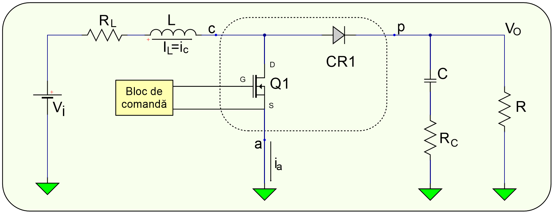 Figure 9. Schematic of a Boost type DC-DC converter.
For analysis, I will use a CAD-type program called LTspice from Analog Devices .
The power switch, \(Q1\), is an N-channel MOSFET transistor, the diode, \(CR1\), is usually a diode that exhibits a low forward voltage drop to minimize losses. The inductor \(L\) and capacitor \(C\) form the output filter.
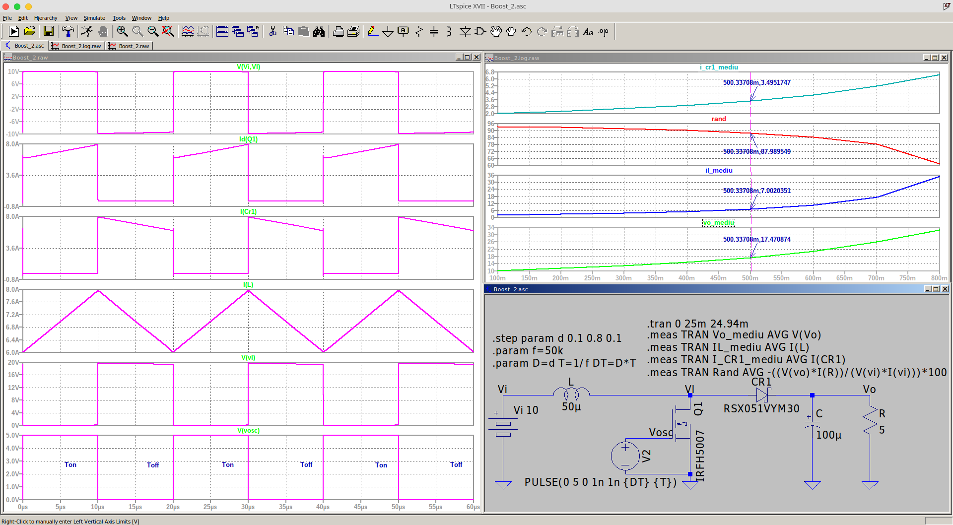 Figure 9a. Schematic of a Buck type DC-DC converter, for simulation with LTspice.
The netlist file of the circuit from Figure 9a is presented below:
* C:\users\florin\Documentele mele\LTspiceXVII\Boost_2.asc
Vi Vi 0 10
M§Q1 Vl Vosc 0 0 IRFH5007
V2 Vosc 0 PULSE(0 5 0 1n 1n {DT} {T})
D§CR1 Vl Vo RSX051VYM30
L Vi Vl 50µ Ipk=7 Rser=0.02 Rpar=38000 Cpar=5.86p mfg="Gowanda" pn="894AT5002V"
C Vo 0 100µ V=25 Irms=370m Rser=0.24 Lser=0 mfg="Nichicon" pn="UPL1E101MPH" type="Al electrolytic"
R Vo 0 5
.model D D
.lib C:\users\florin\Documentele mele\LTspiceXVII\lib\cmp\standard.dio
.model NMOS NMOS
.model PMOS PMOS
.lib C:\users\florin\Documentele mele\LTspiceXVII\lib\cmp\standard.mos
.step param d 0.1 0.8 0.1
.param f=50k
.param D=d T=1/f DT=D*T
.meas TRAN Vo_mediu AVG V(Vo)
.meas TRAN IL_mediu AVG I(L)
.meas TRAN I_CR1_mediu AVG I(CR1)
.meas TRAN Rand AVG -((V(vo)*I(R))/(V(vi)*I(vi)))*100
.tran 0 25m 24.94m
.backanno
.end
During the normal operation of the DC-DC converter, of the Boost type, the switch \(Q1\) is controlled in the closed and open positions by the control circuit/block. This action of the control circuit/block on the switch causes the appearance of a pulse train at the intersection of the three elements \(Q1\), \(CR1\), and \(L\). Even though the inductor \(L\) is connected to the output capacitor, \(C\), only when the diode, \(CR1\), conducts, does it (the inductor) together with the output capacitor, \(C\), form an \(L-C\) output filter aimed at filtering the pulse train to produce a continuous output voltage, \(V_o\).
The analysis in steady state of the DC-DC Boost converter
Such a converter can operate in discontinuous or continuous current mode (depending on the current through the inductor \(L\)).
Continuous current mode is characterized by the continuous flow of current through the inductor \(L\) throughout the entire switching cycle.
Discontinuous current mode is characterized by the interrupted flow of current through the inductor \(L\), with crossings through zero. This mode is characterized by the fact that the current through the inductor is zero for a portion of the switching cycle. It starts from zero, reaches a maximum value, and returns to zero during each switching cycle.
These two modes will be analyzed in detail in the following sections. It is desirable for such a stage to remain in only one mode throughout its operation, as the frequency response of the stage changes significantly between the two operating modes.
For this analysis, an N-channel MOSFET transistor is used, which is controlled by a positive voltage \(V_{GS(ON)}\), applied to the gate \(G\) and source \(S\) of the transistor/switch \(Q1\) by the control circuit that commands this switch/transistor \(Q1\) to the \(ON\) position. The advantage of this N-channel MOSFET transistor is that it has a low conductance resistance \(R_{DS(ON)}\), but the control circuit is more complicated. In the case of a P-channel MOSFET transistor, which generally has a higher conductance resistance \(R_{DS(ON)}\), the control circuit is simpler.
Transistor \(Q1\) and diode \(CR1\) are illustrated in Figure 9, in the box with a dotted line, with terminals labeled a, p, and c. The current through the coil \(L\) denoted as \(I_L\), is the same as the current exiting through the terminal labeled c, namely the current \(i_c\).
The analysis in direct current mode of the DC-DC Boost converter
The operation of the Boost converter in static regime (steady state) in continuous conduction mode (\(I_L>0\)) will be described below.
The main result of this analysis is the dependence of the output voltage \(V_o\) on the duty cycle \(D\) and the input voltage \(V_i\), respectively, conversely, the duty cycle \(D\) can be calculated based on the output voltage \(V_o\) and the input voltage \(V_i\).
The static (steady state) regime implies that the input voltage, output voltage, output current through the load, and duty cycle are fixed and do not vary. In general, uppercase letters are assigned to variable names to indicate a quantity in a static state.
In continuous conduction mode, the Boost converter assumes two switching states during one cycle.
- STATE ON - when the transistor/switch, \(Q1\), is \(ON\) and \(CR1\) is \(OFF\);
- STATE OFF - when the transistor/switch, \(Q1\), is \(OFF\) and \(CR1\) is \(ON\).
A simple linear circuit can represent each state in which the elements \(Q1\) and \(CR1\) are replaced with their equivalent circuits corresponding to each state \(ON\) or \(OFF\).
The equivalent electrical circuits for each state are presented in the figure below, Figure 10.

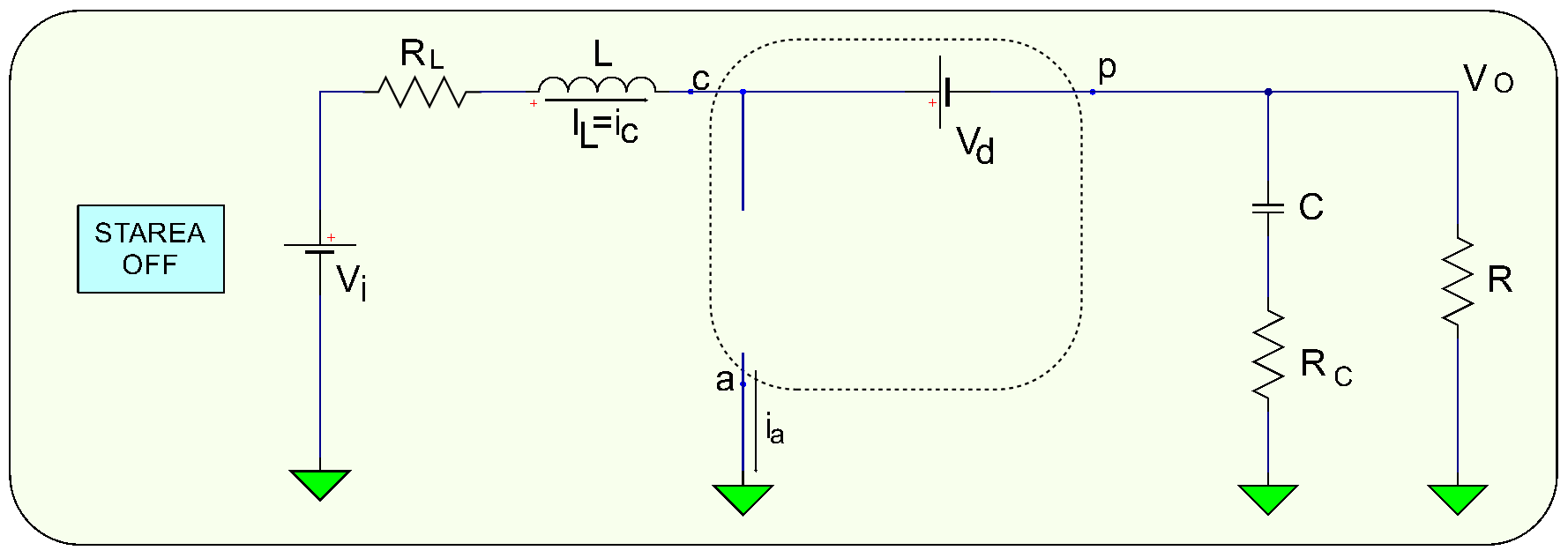
Figure 10. The states \(ON\) and \(OFF\) of the Boost stage.
The duration of the \(ON\) state is:
\[ {T_{ON}}={D} \times {T_S}\]
, where:
\(D\) is the duty cycle, imposed by the control block, expressed as the ratio of the time when the switch is \(ON\) to the total time of the entire period, \(T_S\):
\[ {D} = {{T_{ON}} \over {T_{S}}}\]
The duration of time for the \(OFF\) state is denoted as \(T_{OFF}\). Thus, we have only two states during the duration of a complete cycle (one period) for continuous current mode. The duration of the \(OFF\) state is:
\[ T_{OFF}=(1-D) \times T_S\]
, where:
\((1-D)\) is sometimes denoted as \(D'\).
These time cycles are presented in Figure 11.
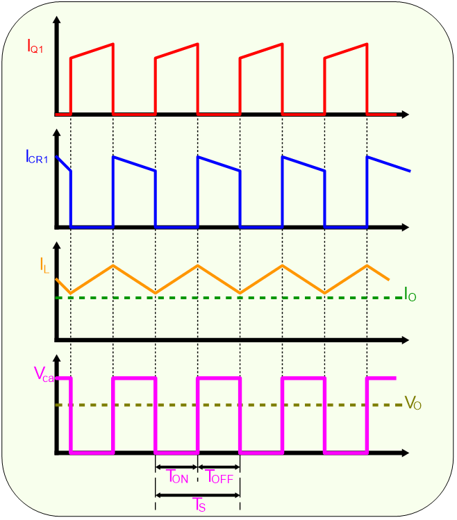
Figure 11. The waveforms in continuous conduction mode, \(I_L>0\).
If we look at Figure 10, during the \(ON\) state, we observe that:
- \(Q1\) exhibits a low resistance, \(R_{DS(ON)}\), from the drain \(D\) to the source \(S\) and has a small voltage drop:
\[ V_{DS}=I_{L} \times R_{DS(ON)}\]
- There is also a small voltage drop across the c.c. resistance of the inductor \(L\), equal to:
\[ V_{RL}=I_L \times R_L\]
Thus, the input voltage \(V_i\), minus the losses (\(V_{DS}+V_{RL}\)), is applied to the left side of the inductor \(L\). \(CR1\) is \(OFF\) during this time because the applied voltage is reverse. The voltage applied to the right side of the inductor \(L\) is the voltage drop across the MOSFET transistor, \(V_{DS}\).
The current through the coil, \(I_L\), flows from the input source, \(V_i\), through \(Q1\) to ground.
During the \(ON\) state, the voltage applied across the coil, \(V_L\), is constant and equal to:
\[ V_L=V_i-V_{DS}- V_{RL}\]
Adopting the polarity convention for the current \(I_L\) presented in Figure 10, the current through the coil increases as a result of the applied voltage. Furthermore, since the applied voltage is essentially constant, the current through the inductor increases linearly.
This increase in the current through the coil during \(T_{ON}\) is illustrated in Figure 11.
\[ {V_L}={L} \times {{di} \over {dt}} \Rightarrow \Delta I_L = {V_L \over L} \times \Delta T \]
The increase in current through the circuit, during the \(ON\) state, is given by:
\[ \Delta I_L(+) = {{V_i - V_{DS} - V_{RL}} \over L} \times T_{ON} \]
The value \(\Delta I_L(+)\) is the ripple of current through the coil. During this period, the entire load current is supplied by the output capacitor, \(C\).
If we look at Figure 10, when \(Q1\) is \(OFF\), it presents a high impedance between the drain \(D\) and the source \(S\). Therefore, since the current flowing through the coil/inductor \(L\) cannot change instantaneously, the current flows from the transistor \(Q1\) to the diode \(CR1\). As the current through the coil decreases, the voltage across the coil reverses polarity until the diode \(CR1\) becomes forward-biased and conducts (\(ON\)).
The voltage on the left side of the inductor, \(L\), remains the same as before being \(V_i-V_{RL}\).
The voltage applied on the right side of the inductor, \(L\), is now the output voltage, \(V_O\), plus the voltage drop, in forward conduction, across the diode, \(V_d\).
The current through the inductor, \(I_L\), now flows from the input source, \(V_i\), through the diode, \(CR1\), to the output formed by the capacitor \(C\) and the load resistance \(R\).
During the \(OFF\) state, the voltage applied to the inductor \(L\) is constant and is equal to:
\[ V_L = (V_O+V_d+V_{RL})-V_i\]
Maintaining the same polarity convention, this applied voltage is negative (or opposite in polarity to the voltage applied in the \(ON\) state).
Therefore, the current through the inductor decreases during the \(OFF\) state.
Also, since the applied voltage is essentially constant, the current through the inductor \(I_L\) will decrease linearly. This decrease in the \(I_L\) current through the inductor during the \(OFF\) state is also presented in Figure 11.
The current through the inductor, during the \(OFF\) state, will decrease according to the relationship:
\[ \Delta I_L(-)={{{(V_O+V_d+V_{RL})-V_i} \over {L}} \times T_{OFF}} \]
The value of \(\Delta I_L(-)\) is also the ripple of current through the inductor.
In steady state, the current \(\Delta I_L(+)\) increases during the \(ON\) state, and the current \(\Delta I_L(-)\) decreases during the \(OFF\) state. These values must be equal. Otherwise, the value of the current will increase or decrease in net values from one cycle to another, and we are no longer in a steady state.
Therefore, these two equations can be equated and solved for \(V_O\) to obtain the output voltage transformation/conversion relationship \(V_O\) for continuous conduction mode.
Solving:
\[ V_O = {(V_i-V_{RL}) \times (1+{T_{ON} \over T_{OFF}})-V_d-V_{DS} \times {T_{ON} \over T_{OFF}}} \]
, where:
\[ \left.\begin{matrix} {T_S=T_{ON}+T_{OFF}} \\ {D={T_{ON} \over T_S}} \\ {(1-D) = {T_{OFF} \over T_S}} \end{matrix}\right\} \Rightarrow V_O={{{V_i-V_{RL}} \over {1-D}}-V_d-V_{DS} \times {D \over {1-D}}}\]
In the equations above for \(\Delta I_L(+)\) and \(\Delta I_L(-)\), the output voltage, \(V_O\), was implicitly assumed to be constant, with no voltage ripple during \(ON\) or \(OFF\).
This is a simplification and involves two separate assumptions:
- First, it is assumed that the output capacitor, \(C\), is sufficiently large so that the ripple/voltage change is negligible;
- Secondly, it is assumed that the voltage drop across \(ESR\) (the equivalent series resistance \(R_C\)) is also negligible.
These assumptions hold true because the value of the voltage ripple is designed to be much smaller than the output voltage, \(V_O\), in c.c..
The relationship of the output voltage transformation factor \(V_O\), as mentioned above, illustrates that the output voltage \(V_O\) can be modified by adjusting the duty cycle factor \(D\) and is always greater than the input voltage \(V_i\) since \(D\) satisfies the condition \(0>D<1\).
Another simplification used is to consider \(V_{DS}\), \(V_d\), and \(R_L\) as implicitly small enough to be ignored, thus:
\[ \left.\begin{matrix} V_{DS}=0 \\ V_d = 0 \\ V_{RL} = 0 \end{matrix}\right\} \Rightarrow V_O = {{V_i} \over {1-D}}\]
A simplified analysis of the circuit is to consider the coil/inductor, \(L\), as an energy storage element.
Thus, when \(Q1\) is \(ON\), energy is added to the coil/inductor, \(L\), and when \(Q1\) is \(OFF\), the inductor/coil, \(L\), and the power source, \(V_i\), deliver energy to the output capacitor, \(C\), and to the load, \(R\).
The output voltage, \(V_O\), is controlled by setting the conduction time of \(Q1\). For example, by increasing the conduction time (the duration of \(ON\)) of \(Q1\), the energy delivered to the inductor/coil, \(L\), will increase, and then more energy will be delivered to the output during the \(OFF\) duration of \(Q1\), which will lead to an increase in the output voltage \(V_O\).
Unlike the buck stage (Buck converter), the average current through the inductor/coil, \(I_{L_{(med)}}\), will not be the same as the output current, \(I_O\), according to Figures 10 and 11.
What is important to remember is that in this case (Boost converter), the coil/inductor, \(L\), provides current to the output only during the \(OFF\) duration. This average current, during a complete switching cycle, is equal to the output current, since the average current through the output capacitor, \(C\), must be zero.
The relationship between the average current through the inductor/coils, \(I_{L_{(med)}}\), and the output current, \(I_O\), of the boost converter operating in continuous regime is given by:
\[ I_{L_{(med)}} \times {T_{OFF} \over T_S} = I_{L_{(med)}} \times (1-D) = I_O \]
or:
\[ I_{L_{(med)}} ={{I_O} \over {1-D}}\]
Another important observation is that the average current through the inductor, \(I_{L_{(med)}}\), is proportional to the output current, \(I_O\).
For example, if the current through the coil/inductor, \(I_{L_{(med)}}\), decreases by \(2[A]\) due to the reduction in load current, then the minimum values, \(\Delta I_L(-)\), and maximum values, \(\Delta I_L(+)\), of the current through the coil/inductor also decrease by \(2[A]\), assuming that continuous conduction mode is maintained.
The analysis in discontinuous current mode of the c.c. - c.c. boost converter raises.
In the following, we will analyze what happens when the current through the load is low and the conduction mode changes from continuous conduction mode to discontinuous conduction mode. We remind that for continuous conduction mode, the current through the inductor/coil, \(I_{L(med)}\), follows the output current, \(I_O\), and if the latter decreases, then the average current through the inductor/coil, \(I_{L(med)}\), will do the same. Furthermore, both the minimum and maximum peaks of the inductor current will follow the average current of the coil/inductor, \(I_{L(med)}\).
If the current through the output load is reduced below the critical level, the current through the inductor will be zero for a portion of the switching cycle. This should be evident from the waveforms presented in Figure 11, as the peak-to-peak amplitude of the current ripple \(\Delta I_L\) does not change with the output current through the load. In a Boost converter/stage, if the current through the inductor \(I_L\) tries to drop below zero, it will stop at zero (due to the unidirectional flow of current through the diode \(CR1\)) and will remain there until the beginning of a new switching cycle.
This operating mode is called discontinuous conduction mode. A Boost converter/stage operating in this discontinuous conduction mode has three unique states during each switching cycle, unlike the two states for continuous conduction mode.
The state of the current through the inductor/coils, \(I_L\), when the Boost converter/stage is at the boundary between continuous and discontinuous conduction mode is shown in Figure 12. It can be observed how the current through the inductor decreases to zero and the next switching cycle begins immediately after the current reaches zero.
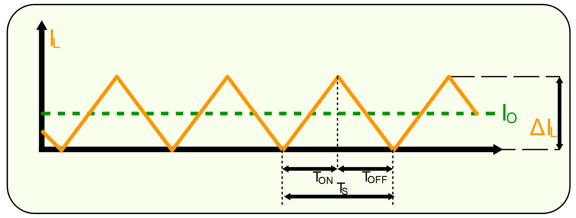
Figure 12. The boundary between continuous conduction mode and discontinuous conduction mode.
Further reduction of the output current puts the Boost converter into discontinuous conduction mode. This conduction mode is illustrated in Figure 13. The frequency response of the Boost converter in discontinuous conduction mode is quite different from the frequency response in continuous conduction mode. Additionally, the input-output relationship is quite different, as shown below.
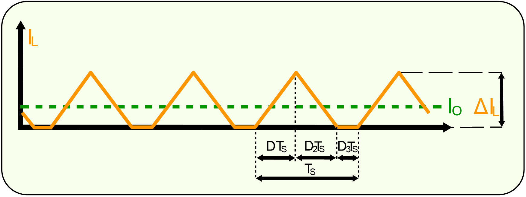
Figure 13. Discontinuous conduction mode.
Before determining the conversion ratio of the discontinuous conduction mode, we note that there are three unique states that the Boost converter realizes during operation in the discontinuous current mode:
- The \(ON\) state is when \(Q1\) is \(ON\) and \(CR1\) is \(OFF\);
- The \(OFF\) state is when \(Q1\) is \(OFF\) and \(CR1\) is \(ON\);
- The \(IDLE\) state is when \(Q1\) is \(OFF\) and \(CR1\) is \(OFF\);
The first two states are identical to those of the continuous conduction mode, and the circuits in Figure 10 are applicable except for \(T_{OFF} \neq (1-D) \times T_S\). The remaining time is the \(IDLE\) state. Additionally, we will be able to omit: the resistance in c.c. \(R_L\) of the coil/inductor \(L\) implicitly and the voltage drop across it \(V_{RL}\), the voltage drop across the diode \(V_d\), and the voltage drop \(V_{DS}\) across the transistor \(Q1\) in the \(ON\) state, as they are small enough to be considered zero.
The duration of the \(ON\) state is:
\[ T_{ON} = D \times T_S\]
, where:
\(D\) represents the duty cycle set by the control circuit, expressed as the ratio of \(T_{ON}\) to the duration of a complete cycle \(T_S\), namely:
\[ D = {T_{ON} \over T_S}\]
The duration of the \(OFF\) state is:
\[ T_{OFF} = D_2 \times T_S\]
The duration of the \(IDLE\) state is the remainder of the switching time and is:
\[ T_S-T_{ON}-T_{OFF} = D_3 \times T_S\]
these states are presented in Figure 14.
The equations for the increase of current, \(\Delta I_L(+)\), through the coil/inductor \(L\) during the \(ON\) state and the equations for the decrease of current, \(\Delta I_L(-)\), through the coil/inductor \(L\) during the \(OFF\) state are determined as follows.
Thus, the increase of current \(\Delta I_L(+)\) through the coil/inductor \(L\), during the \(ON\) state, is given by:
\[ \Delta I_L(+)={V_i \over L} \times {T_{ON}} = {V_i \over L} \times {D \times T_S} = I_{pk} \]
The magnitude of the current ripple, \(\Delta I_L(+)\), also represents the peak current, \(I_{pk}\), since in discontinuous conduction mode, the current starts from zero at the beginning of each cycle.
The decrease in current \(\Delta I_L(-)\) through the coil/inductor \(L\), during the \(OFF\) state, is given by:
\[ \Delta I_L(-)={{V_O-V_i} \over L} \times {T_{OFF}}={{{V_O - V_i} \over L} \times D_2 \times T_S} \]
As in the case of continuous conduction mode, the current increases, \(\Delta I_L(+)\), during the \(ON\) duration and the current decreases \(\Delta I_L(-)\) during the \(OFF\) duration, and these increases and decreases in current are equal.
Therefore, these two equations can be equated and solved for \(V_O\), to obtain the first of the two equations that must be used to derive/solve the voltage conversion ratio:
\[ V_O=V_i \times {{T_{ON} + T_{OFF}} \over {T_{OFF}}}=V_i \times {{D+D_2} \over {D_2}} \]
The output current, \(I_O\), which represents the output voltage \(V_O\) divided by the output load \(R\), is:
\[ I_O={V_O \over R} = {{1 \over T_S} \times \left({1 \over 2} \times I_{pk} \times D_2 \times T_S \right)} \]
Substituting in the equation above \(I_{pk}\) determined earlier, will result in:
\[ I_O={V_O \over R}={ {1 \over T_S} \times \left[ {1 \over 2} \times \left( {V_i \over L} \times D \times T_S \right) \times D_2 \times T_S \right]} \]
\[ I_O={V_O \over R}={{V_i \times D \times D_2 \times T_S} \over {2 \times L}} \]
Thus, we have obtained two equations, one for the output current, \(I_O\), and one for the output voltage, \(V_O\), both with the terms \(V_i\), \(D\), and \(D_2\).
Now solving each equation for \(D_2\) and equating the two obtained equations. The resulting equation will be an expression for the output voltage, \(V_O\).
The voltage conversion/transformation relationship in discontinuous conduction mode is given by:
\[ V_O=V_i \times {{1+ \sqrt {1+{{4 \times D^2} \over K}}} \over 2} \]
, where:
\[ K = {{2 \times L} \over {R \times T_S}} \]
The above relationship presents one of the major differences between the two conduction modes. For discontinuous conduction mode, the transformation/conversion relationship of the output voltage, \(V_O\), is a function of the input voltage, \(V_i\), the duty cycle, \(D\), the inductance \(L\), the switching frequency \(T_S\), and the load resistance \(R\), while for continuous conduction mode, the transformation/conversion relationship of the output voltage depends only on the input voltage, \(V_i\), and the duty cycle, \(D\).

Figure 14. Waveforms in discontinuous conduction mode
In typical applications, the Boost converter operates either in continuous conduction mode or in discontinuous conduction mode. For a specific application, a single operating mode is chosen, and the stage is designed to maintain that mode.
In the following section, we will determine the necessary relationships for selecting the coil/inductor that will allow the circuit to operate in a single conduction mode.
Critical inductance
The previous analyses of the Boost converter were for continuous and discontinuous conduction modes in static regime.
The conduction mode of the stage is a function of the input voltage, output voltage, output current, and the inductance value of the output coil.
A Boost stage can be designed to operate in continuous mode for load currents above a certain level, usually 5%-10% of the maximum value.
Typically, the input voltage range, output voltage, and load current are imposed (defined) parameters of the Boost stage, while the value of the inductor is a parameter that will be determined in order to maintain the continuous operating environment.
The minimum value of the inductor to maintain continuous conduction mode can be determined by following the subsequent algorithm.
To begin with, we define \(I_{O(crit)}\) as the minimum current for which continuous operation can still be maintained, as shown in Figure 12.
\[ I_{L(min-average)}= {{\Delta I_L} \over {2}} \]
After which we determine the minimum inductance of the coil/inductor that satisfies the above relationship, as follows:
\[ L_{min} \geq {1 \over 2} \times (V_i+V_{DS}-V_{RL}) \times {T_{ON} \over I_{L(min)}} \]
The above equation can be simplified and arranged in a more usable form:
\[ L_{min} \geq {{V_O \times T_S} \over {16 \times I_{O(crit)}}} \]
Using the inductance value thus calculated ensures operation in continuous mode for load/output currents above the critical current level, \(I_{O(crit)}\).
Calculation of components for a Boost stage
The following will present an algorithm for calculating the sizing of a Boost stage that will operate in continuous conduction mode.
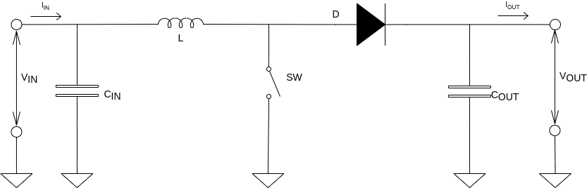
Figure 15. Schematic diagram of a Boost stage
Necessary parameters (known)
In order to size a Boost stage (as shown in the figure above), the following four parameters are required:
- \(V_{IN_{(min)}}\) and \(V_{IN_{(max)}}\), the input voltage range;
- \(V_{OUT}\), the output voltage;
- \(I_{OUT_{(max)}}\), the maximum output current;
- The datasheet of the IC (integrated circuit) used in the construction of the Boost stage, from which certain parameters will be utilized.
Determining the maximum switching current
To determine the maximum switching current, it is first necessary to determine the duty cycle \(D\) for the minimum input voltage, as this imposes the maximum switching current:
\[ D={1-{{V_{IN_{(min)}} \cdot \eta} \over V_{OUT}}} \]
where:
\(V_{OUT}\) - represents the output voltage;
\(V_{IN_{(min)}}\) - represents the minimum input voltage;
\(\eta\) - represents the efficiency of the Boost stage.
It is necessary to take into account the efficiency, \(\eta\), to cover the losses of the Boost stage. When this is not known, from the datasheets, it can be estimated that if we consider an efficiency of 85%, we will cover the losses within the Boost stage.
The next step in determining the maximum switching current is to determine the current ripple through the inductor. In the datasheet of the converter, the specific value of the inductor is normally specified, or a series of inductors that can be used in the application of the IC (integrated circuit).
In determining the current ripple (ripple current) through the inductor, we will use the inductance value from the middle of the recommended range, or if this parameter is not specified, we will use the value determined in the next section - Choosing the Inductor.
\[ \Delta I_L = {{{V_{IN_{(min)}}} \cdot D} \over {f_s \cdot L}} \] where: **$V_{IN_{(min)}}$** - represents the minimum input voltage; **$D$** - duty cycle, determined previously; **$f_s$** - the minimum switching frequency of the converter; **$L$** - the value of the inductor's inductance. The following will determine whether the integrated circuit (IC) containing **$SW$** can provide the maximum output current (switching current). \[ I_{MAXOUT} = {(I_{LIM_{(min)}}-{\Delta I_L \over 2}) \cdot (1-D)} \]
where:
\(I_{LIM_{(min)}}\) - represents the minimum value of the limit current associated with the switching element \(SW\), from the catalog data;
\(\Delta I_L\) - represents the current ripple, calculated previously;
\(D\) - represents the duty cycle, calculated previously.
If the calculated value of the maximum output current, \(I_{MAXOUT}\), is less than the required maximum output current, then we will increase the switching frequency, \(f_s\), to reduce the current ripple, \(\Delta I_L\), or a switch with a higher output current will be chosen. If the maximum output current, \(I_{MAXOUT}\), is only slightly less than the required maximum output current, then we will increase the inductance of the coil/inductor, \(L\), if we are within the recommended range of the inductor. It can be observed from the previous equation of the current ripple \(\Delta I_L\) that by increasing the inductance, \(L\), or increasing the switching frequency, \(f_s\), the current ripple \(\Delta I_L\) can be reduced, and consequently, the maximum output current, \(I_{MAXOUT}\), will increase.
If the calculated value of the maximum output current, \(I_{MAXOUT}\), exceeds the maximum required output current, then the maximum switching current, \(I_{SW_{(max)}}\), will be calculated using the formula:
\[ I_{SW_{(max)}} = {{\Delta I_L \over 2} + {I_{OUT_{(max)}} \over {1-D}}} \]
where:
\(\Delta I_L\) - represents the current ripple through the coil/inductor;
\(I_{OUT_{(max)}}\) - represents the maximum current required at the output;
\(D\) - represents the duty cycle;
\(I_{SW_{(max)}}\) - represents the maximum switching current, which is the peak current that the switch element, \(SW\), the inductor, \(L\), and the diode, \(D\), must withstand.
Choosing the inductor
The datasheets for the Boost type converter often provide a series of recommended values for the inductor. In this case, we can choose the coil/inductor to have an inductance value from the list of values or a specific model indicated.
From the previous formulas, it can be concluded that the higher the inductance value of the coil/inductor, \(L\), the higher the maximum output current value, \(I_{MAXOUT}\), due to the reduction of the current ripple, \(\Delta I_L\). Additionally, the maximum current supported by the chosen coil/inductor, \(L\), must be greater than the maximum switching current value, \(I_{SW_{(max)}}\).
For cases where a specific list of coils/inductors is not provided in the datasheets, the following equation can be used to select the required inductance:
\[ L={{V_{IN} \cdot (V_{OUT} - V_{IN})} \over {\Delta I_L \cdot f_s \cdot V_{OUT}}} \] where: **$V_{IN}$** - represents the input voltage; **$V_{OUT}$** - represents the output voltage; **$f_s$** - represents the switching frequency of the converter; **$\Delta I_L$** - represents the estimated ripple current through the inductor. Since in this case we do not know **$L$** and cannot determine **$\Delta I_L$** using the previous formula, we will estimate it as: \[ \Delta I_L={(0.2 \div 0.4) \cdot I_{OUT_{(max)}} \cdot {V_{OUT} \over V_{IN}}} \] where: **$\Delta I_L$** - represents the estimated ripple current through the inductor; **$I_{OUT_{(max)}}$** - represents the maximum current required at the output; **$V_{OUT}$** - represents the output voltage; **$V_{IN}$** - represents the input voltage. ### Choosing the diode To reduce losses, Schottky diodes will be used. The diode must have a forward conduction current, **$I_F$**, equal to the maximum output current: \[ I_F={I_{OUT_{(max)}}}\]
where:
\(I_F\) - represents the average value of the diode's forward conduction current;
\(I_{OUT_{(max)}}\) - represents the maximum current required at the output.
The chosen Schottky diode must have a peak current greater than the average value.
Another parameter that will need to be calculated is the power dissipated by the diode, \(P_D\), as follows:
\[ P_D={I_F \cdot V_F}\]
where:
\(I_F\) - represents the average value of the diode current in forward conduction;
\(V_F\) - represents the voltage drop across the diode in forward conduction.
The value of the output voltage
In approximately all voltage converters (integrated circuits), the output voltage is set using a resistive divider (which is integrated in the case of fixed output voltage converters).
The voltage divider can be calculated using the feedback voltage and current, \(V_{FB}\) and \(I_{FB}\), respectively.
Figure 16. The resistive divider used to set the output voltage
The current through the resistive resistor, \(I_{R12}\), must be at least 100 times greater than the feedback current, \(I_{FB}\):
\[ I_{R12} \geq {100 \cdot I_{FB}}\]
where:
\(I_{FB}\) - represents the feedback current, established according to the catalog data;
\(I_{R12}\) - represents the current through the resistive divider to ground.
This constraint ensures that we achieve an error of less than \(1\%\) in voltage measurement, and the feedback current, \(I_{FB}\), can be neglected.
Considering the previous constraint, the resistors will be calculated as follows:
\[ R_2={V_{FB} \over I_{R12}}\]
\[ R_1={R_2 \cdot \left({V_{OUT} \over {V_{FB}}}-1 \right)}\]
where:
\(R_1\), \(R_2\) - represent the resistances of the voltage divider;
\(V_{FB}\) - represents the feedback voltage, from the datasheet;
\(I_{R12}\) - represents the current through the resistive resistor;
\(V_{OUT}\) - represents the required output voltage.
Choosing the input capacitor
The minimum value for the input capacitor is normally given by the converter's datasheet.
This minimum value is necessary to establish the input voltage due to the peak current requirement of the switching source.
The best are capacitors with low equivalent series resistance, \(ESR\), and ceramic capacitors belong to this category.
If the input voltage is noisy, this capacitance can be increased.
Choosing the output capacitor
And in this case, we will choose the capacitor with low \(ESR\), and ceramic capacitors are a good choice in this regard.
If the converter is equipped with an external capacitor, then any capacitance value above the minimum recommended value from the datasheets can be used.
The following equations can be used to select the output capacitor for a desired voltage ripple:
\[ C_{OUT_{min}}={{I_{OUT_{(max})} \cdot D} \over {f_s \cdot \Delta V_{OUT}}} \]
where:
\(C_{OUT_{min}}\) - represents the minimum capacitance of the output capacitor;
\(I_{OUT_{(max})}\) - represents the maximum output current;
\(D\) - represents the duty cycle;
\(f_s\) - the minimum oscillation frequency of the converter;
\(\Delta V_{OUT}\) - voltage ripple at the output.
\(ESR\) adds even more ripple, given by the equation:
\[ \Delta V_{OUT_{ESR}}={ESR \cdot \left( {{I_{OUT_{(max})} \over {1-D}}+{{\Delta I_L} \over 2}}\right)} \]
where:
\(\Delta V_{OUT_{ESR}}\) - the voltage ripple contribution due to \(ESR\);
\(ESR\) - the equivalent series resistance associated with the capacitor;
\(D\) - represents the duty cycle, calculated previously;
\(\Delta I_L\) - represents the ripple current through the inductor, determined previously.